![[Translate to English:] Laser-Mikrobearbeitung - Höchste Präzision](/fileadmin/_processed_/7/c/csm_Imagebild_Laserabtrag3_83932edea1.jpg "[Translate to English:] Laser-Mikrobearbeitung - Höchste Präzision")
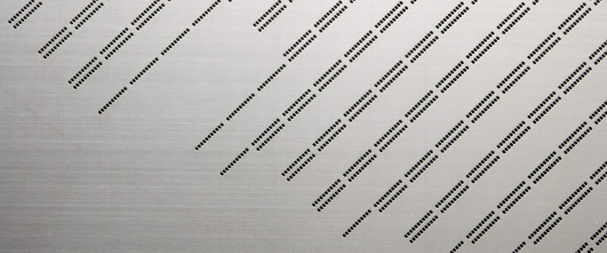
Wafer bumping - stencil
Laser cut stainless steel stencil for solder paste printing on wafer
Wafer bumping stencils are characterized by a high number of apertures which lie close together in the size of 90µm x 110µm. A package density of up to 250000 openings is not unusual. The thickness of a Wafer bumping - stencil is typically between 20 to 75µm. Due to this high package density and due to the small openings high requirements on the precision of the laser cut process and the positioning accuracy are recommended.
The wafer bumping - stencil is influencing a lot the amount of solder and therefore the height of the bumps. The Wafer bumping - stencil from LaserJob guarantees through particularly close tolerances in material thickness of ±3µm and an aperture outline tolerance of ±3µm an ideal consistency of the transferred solder paste and has thereby clear advantages in relation to other manufacturing processes.
LaserJob developed a special laser cut process for the Wafer bumping - stencil which guarantees a high precision and fulfils the high requirements of the component manufacturers. A special treatment of the bottom side of the stencil is needed to avoid damages on the wafer due to smallest unevenness. Therefore the squeegee side and bottom side of the stencil are treated with an ultrafine brush to guarantee a defined surface roughness of <0,9µm.


